Capacitors · Volume 4
How Capacitors Are Made — Then and Now
4.1 The one idea behind every capacitor
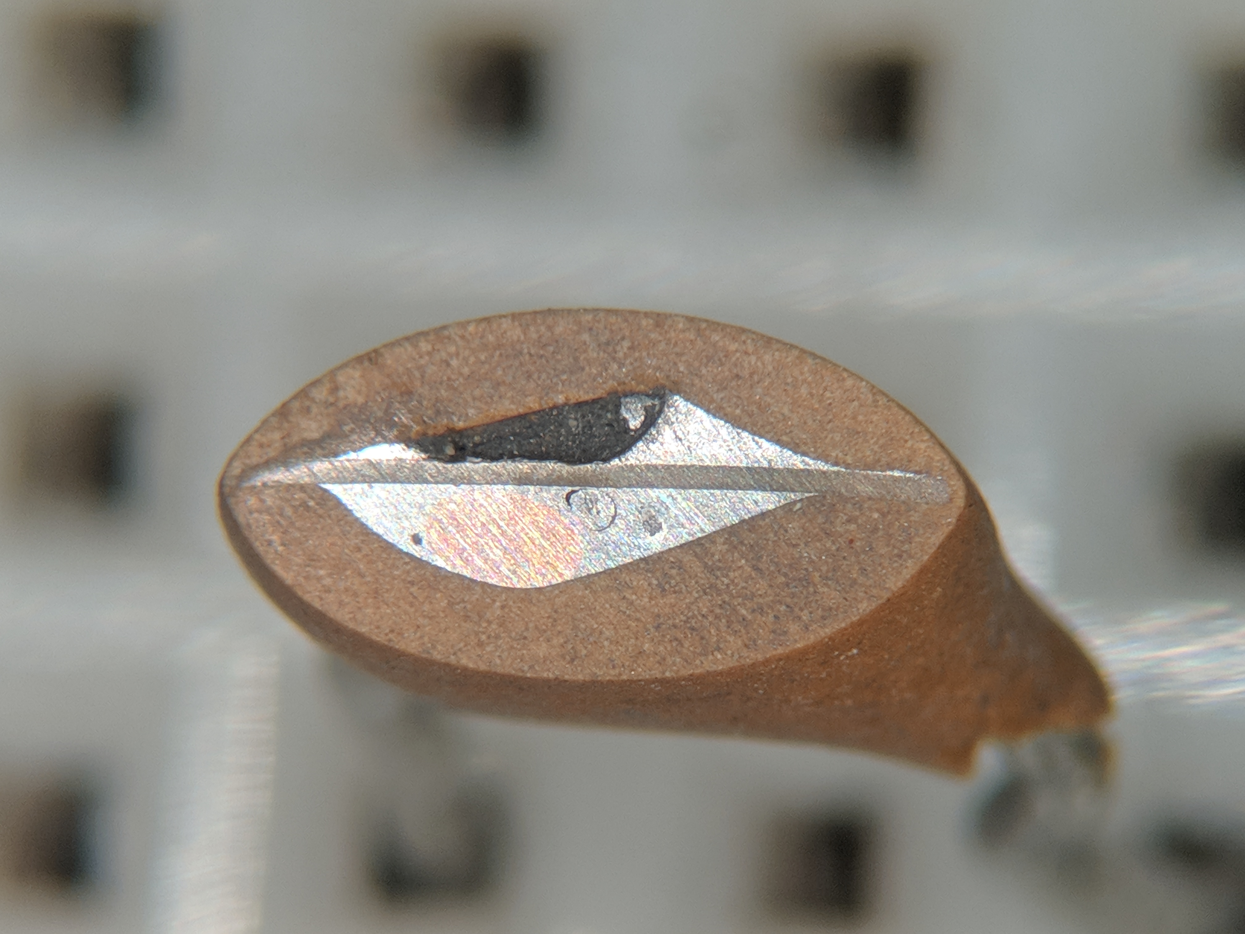
Strip away the packaging and every capacitor ever built is the same sentence: a conductor, a thin insulator, and a second conductor, arranged so that the two conductors face each other across as much area as possible with as little insulator between them as the maker can get away with. The physics volumes in this family explain why that arrangement stores charge and how the dielectric earns its keep; this volume is about the far less glamorous question of how a factory actually builds the thing — and how the answer changed from a person at a bench winding waxed paper by hand to a machine placing components the size of a grain of sand by the million per hour.
The whole art of capacitor manufacture is contained in that opening sentence, because the two demands in it pull against each other. More area means more capacitance, so makers want vast electrode area folded into a tiny package. Thinner dielectric also means more capacitance (and, usefully, more capacitance for a given voltage of headroom), so makers want the insulator as thin as physics and their yield will allow. But area folded tightly invites shorts, and a dielectric made thinner is a dielectric closer to breaking down. Every process described below is a different clever answer to the same problem: maximise electrode area and minimise dielectric thickness, at acceptable yield, for the least money. The technologies look wildly different — a wound cylinder of plastic, a fired brick of ceramic, a sponge of tantalum, a can of etched foil and electrolyte — but they are all solving that one optimisation, and once the reader sees the optimisation the zoo of construction styles turns into a small number of recurring tricks.
Three of those tricks are worth naming up front, because they show up again and again. The first is rolling: take two long ribbons of conductor and two of insulator, and wind them into a cylinder so that a huge facing area lives in a small volume. The second is stacking: interleave many short layers of conductor and insulator into a block, which does the same thing without the geometry of a spiral. The third — the cleverest — is growing or roughening the surface itself: instead of relying on flat foil, explode the metal’s surface into a labyrinth of pits or a porous sponge, then grow an insulating skin only a few atoms thick directly on that enormous surface. Electrolytics and tantalums live entirely by the third trick, which is why they pack so much capacitance into so little space and why they behave so differently from the rolled and stacked types. With those three ideas in hand, the factory tour begins where the industry itself began: with a roll.
4.2 The rolled cylinder: the classic form
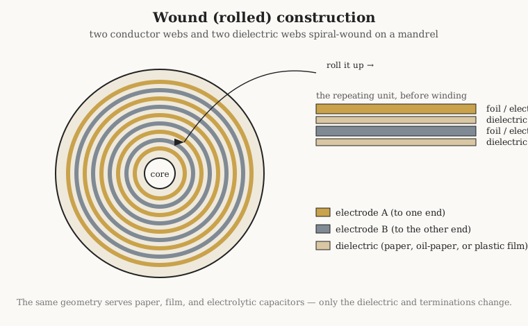
For the first half of the twentieth century, and still today for film and electrolytic types, the default capacitor was a wound cylinder. The recipe is exactly the opening sentence rendered as ribbons: lay down a strip of metal foil, a strip of dielectric, a second strip of foil, a second strip of dielectric, and wind the four-ply sandwich onto a mandrel — a spindle — until it becomes a compact roll. The two foils never touch; the two dielectric webs keep them apart through every turn of the spiral. Unrolled, a single small capacitor’s foils can run to a remarkable length, which is the whole point: winding is simply a way to store a large flat area in a cylinder that fits on a circuit board.
4.2.1 Waxed paper and foil: the old way
The original dielectric web was paper — literally tissue-thin kraft paper — and the original electrode was tin or aluminium foil. Paper on its own is porous and hygroscopic, a poor and unstable insulator, so the wound element was dried and then impregnated: soaked in molten wax, or later in mineral oil or a synthetic oil, to drive out moisture and fill the paper’s pores with something that would not conduct. The result was the wax- or oil-paper capacitor that fills every pre-1960 radio and amplifier — the “condenser” of the old schematics. The paper volume in this family covers why these parts fail so reliably with age (the seals let moisture back in and the leakage current climbs until the capacitor is really a leaky resistor), but the manufacturing point here is simpler: the whole thing was assembled wet, sealed, and prayed over. Tolerances were loose, the parts were bulky, and a skilled operator wound them one or a few at a time.
Paper’s replacement was plastic film, and that single substitution — a web of extruded, biaxially stretched polymer instead of a web of paper — is most of the story of the modern film capacitor. Plastic films can be made far thinner than paper, are not hygroscopic, insulate more predictably, and can be manufactured to tight thickness control. The two that dominate are polyester (PET, sometimes called Mylar) and polypropylene (PP); PET has the higher permittivity, so it packs more capacitance into a given volume, while PP has lower loss and better behaviour at high frequency and high ripple, which is why the film volume sends you to PP for snubbers and motor-run duty and to PET for cheap, compact general coupling.
4.2.2 Film-and-foil versus metallized film
Once the dielectric became plastic, the industry split the electrode question two ways, and the split still defines film capacitors today. In film-and-foil construction, the electrodes are still separate sheets of real metal foil, wound with the plastic film exactly as the old paper-and-foil parts were. This gives a robust, low-resistance electrode able to carry large currents, at the cost of bulk.
In metallized-film construction, the separate foil disappears. Instead, one face of the plastic film is coated with a vanishingly thin layer of metal — typically aluminium or zinc — deposited by evaporating the metal in a vacuum and letting the vapour condense onto the moving film. “Metallized” simply means the electrode is a vapour-deposited coating on the dielectric itself, rather than a free-standing sheet. Two metallized films (or a metallized film wound with a plain one) then make the capacitor. The coating is measured in tens of nanometres — thousands of times thinner than any foil — so the finished part is dramatically smaller and lighter.
The thinness buys something better than size, though: self-healing. When a weak spot in the dielectric finally breaks down and a tiny arc punches through, the intense local current dumps enough heat to vaporise the feather-thin metal coating in a small ring around the fault. The electrode simply evaporates away from the puncture, isolating it; the short clears itself in microseconds and the capacitor keeps working, slightly smaller in capacitance and none the worse. Published figures put the energy to clear one fault in the rough range of a tenth of a joule. A film-and-foil part cannot do this — its thick foil has nowhere near enough resistance to vaporise locally, so a puncture stays a short. This is the manufacturing reason metallized film became the default for anything on the AC mains, where the “clearing” mechanism turns a would-be catastrophic short into a self-repair, and it is why the safety-rated X and Y capacitors the film volume discusses are built this way.
4.2.3 Getting current in and out: tabs versus extended foil
A wound element is useless until its two electrodes are connected to leads, and how that connection is made turns out to matter enormously for performance. The crude method is the inserted tab: during winding, a metal strip is laid against each foil and brought out of the roll, and the leads attach to the tabs. It works, but every bit of current entering the electrode must funnel through the one narrow strip, which adds resistance and inductance.
The better method is extended foil. The two electrodes are wound offset — one foil juts slightly past the dielectric at one end of the cylinder, the other juts past at the opposite end. Now each electrode presents a bare metal edge, a spiral of exposed foil, at its own end of the roll. That edge is then contacted all at once by spraying molten metal onto it — a technique called schoopage, after the Swiss engineer Max Schoop who invented the metal-spray process; in the trade it is simply the “end spray” or “schoop.” The sprayed cap welds every turn of the spiral together and gives the lead a low-resistance, low-inductance connection across the full width of the electrode.
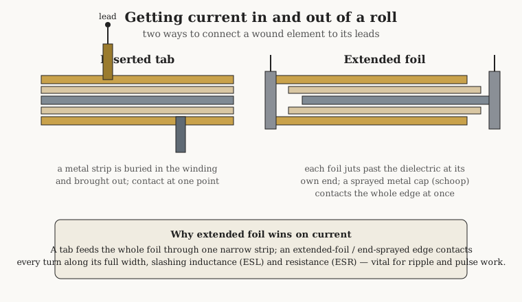
The difference is not cosmetic. The equivalent-series-resistance and equivalent-series-inductance that the real-capacitor volume dwells on are largely set right here, at the terminations; an extended-foil, end-sprayed part can carry ripple and pulse currents that would cook a tabbed one. After termination the cylinder is often pressed flat into an oval cross-section — flattening both saves board space and, by shortening the current path across the winding, trims inductance further — then taped, boxed, or potted in resin and marked. The same wound-and-flattened element, with a different dielectric and different end treatment, is the physical heart of both the film capacitor and the aluminium electrolytic; the geometry is that general.
4.3 Ceramic disc: the simplest survivor
Not every capacitor is rolled. The oldest ceramic construction is almost aggressively simple: a single flat wafer of ceramic, a millimetre or so across, with a conductive silver coating fired onto each face. The two silvered faces are the electrodes; the ceramic between them is the dielectric. Leads are soldered to the two faces, and the whole thing is dipped in a protective coating of phenolic resin or epoxy — the familiar orange or blue lentil hanging off two wires in any older circuit. That is the entire capacitor: one layer of the opening sentence, made tangible.
Disc capacitors are cheap, tolerant of abuse, and still made by the billion for undemanding jobs, but a single layer can only offer so much capacitance — area is limited to the size of the disc, and the ceramic can only be made so thin before it becomes fragile. The obvious way to get more is to stack many such layers in parallel, and doing exactly that, at a scale and precision the disc-makers of the 1930s could not have imagined, produced the single most important capacitor of the modern era.
4.4 The multilayer ceramic chip: the crown jewel
The multilayer ceramic capacitor — MLCC — is the component the electronics industry now consumes in the trillions per year. Open any phone, laptop, or car module and the great majority of the small rectangular parts on the board are MLCCs. Every one is the disc capacitor’s idea taken to an extreme: not one silvered wafer but a monolithic block containing hundreds of interleaved ceramic and metal layers, fused into a single ceramic brick smaller than a match head. The process that makes them is a genuinely beautiful piece of manufacturing, and it deserves the space.
4.4.1 Tape casting the green sheet
It begins as a liquid. Fine ceramic powder — barium titanate for the high-permittivity Class II types, or a lower-permittivity formulation for the stable Class I types the ceramic volume distinguishes — is milled together with organic binders, plasticisers, and solvents into a smooth slurry with the consistency of paint. That slurry is tape cast: pumped onto a moving polymer carrier film and drawn out beneath a precision blade called a doctor blade, which meters it into a wet layer of exact thickness. The solvent flashes off and leaves a flexible, leathery sheet of binder-held ceramic powder — “green” ceramic, meaning unfired — which can be handled and printed like a strip of film. The thickness of that cast sheet is the single most important number in the whole process, because it will become the dielectric layer between two electrodes, and it is the parameter the entire industry has spent forty years driving down.
4.4.2 Screen-printing the electrodes
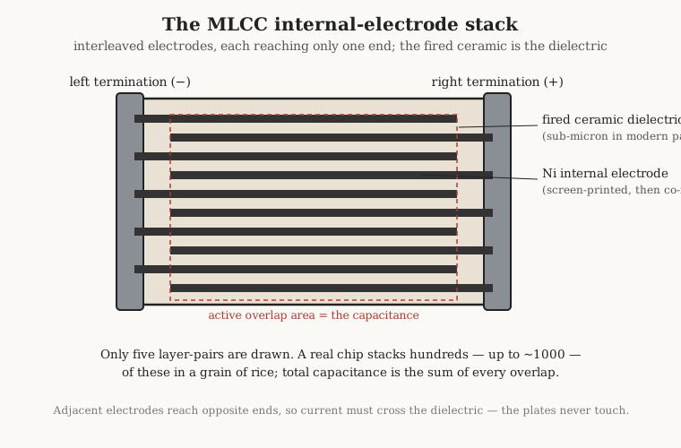
The green sheet then passes under a screen printer, which lays down the internal electrode as a pattern of metal-bearing ink — a paste of fine metal powder in an organic vehicle — printed onto the ceramic exactly the way a T-shirt is screen-printed. The pattern is not a solid coat but an array of electrode rectangles, offset so that when the layers are later stacked, alternate electrodes will reach out to opposite ends of the finished chip. This is the same interleaving as the extended-foil roll, done flat: every electrode connects to one end only, and the plates that face each other across a ceramic layer always belong to opposite ends.
Which metal goes into that paste is one of the great stories of the industry. For decades the internal electrodes had to be a precious metal — palladium, or a palladium-silver alloy — because base metals like nickel would simply oxidise into a non-conductor at the ferocious temperatures the ceramic needs to be fired. As MLCCs multiplied and layer counts climbed, the palladium content became an eye-watering fraction of the cost. The escape was the base-metal electrode (BME) transition, worked out through the 1990s and rolled out broadly in the 2000s: reformulate the ceramic and fire it in a carefully controlled reducing atmosphere — starved of oxygen — so that cheap nickel electrodes survive the firing without oxidising. BME did to the MLCC’s cost structure what the transistor did to the vacuum tube’s, and essentially all high-volume MLCCs today use nickel internal electrodes with fired-on copper terminations.
4.4.3 Stacking, pressing, and dicing
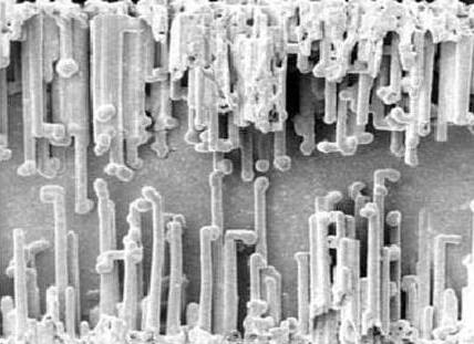
The printed sheets are cut and stacked, layer upon layer, in a jig that keeps the offset electrode pattern in perfect register — a printed sheet, another on top with its electrodes shifted to the opposite end, another shifted back, and so on for however many layers the design calls for. A modern high-capacitance chip may stack several hundred such layers, and the highest approach the order of a thousand. Cover layers of plain ceramic go on top and bottom. The whole stack is then pressed under heat and high pressure, which welds the green layers into one coherent laminated bar with no air trapped between them. That bar is diced — sawn or cut on a grid into thousands of individual green chips, each now a tiny laminated block with electrode edges exposed on two opposite faces where the cut passed through them.
4.4.4 Binder burnout and co-firing
The green chips are still mostly organic binder, and firing them straight into a hot furnace would let that binder erupt into gas and crack them apart. So they first go through binder burnout (debinding), a slow, gentle bake that oxidises and drives off the organics without disrupting the delicate structure. Then comes the event the whole process is built around: co-firing. The chips are sintered at high temperature — broadly in the range of 1100 to 1300 °C for barium-titanate dielectrics, in the oxygen-starved atmosphere the nickel electrodes require — and in that furnace two things happen at once. The ceramic powder densifies and its grains grow together into a solid, dense, gas-tight ceramic; and the metal powder in the printed electrodes sinters into continuous metal films. Ceramic and metal, dielectric and electrode, fuse together in the same fire into a single monolithic object. That simultaneous firing — hence co-firing — is what makes the MLCC a solid ceramic brick rather than a glued-up stack, and it is the reason the part is so mechanically and thermally robust.
4.4.5 Termination and plating
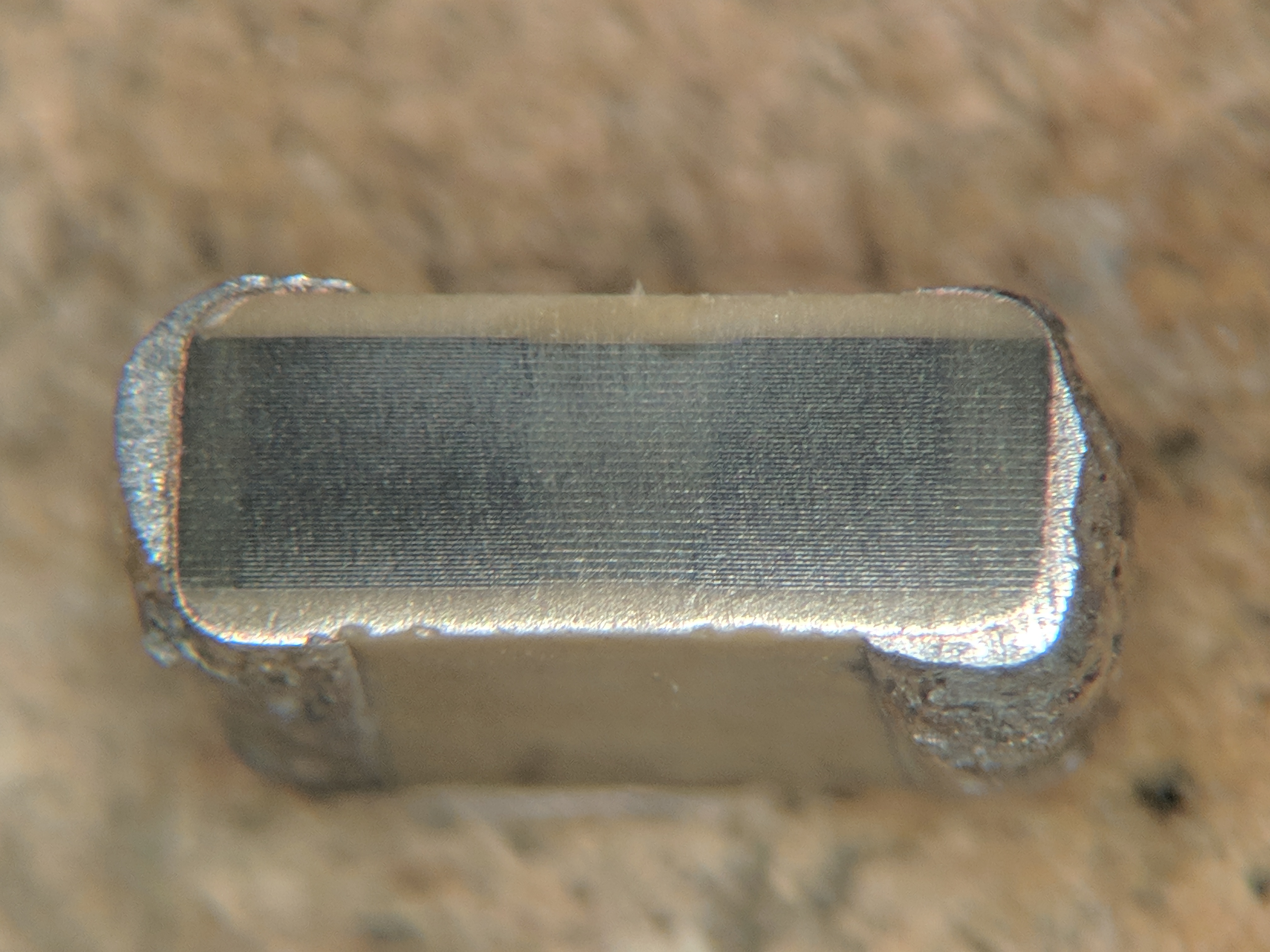
Firing leaves the interleaved electrodes exposed at the two cut ends, one polarity’s electrodes at each end. A metal termination paste — typically copper — is dipped onto each end and fired so that it contacts every one of that end’s electrode edges at once, exactly as the schoop cap contacts a wound element. The fired termination is then electroplated, usually with a barrier layer of nickel and a finish of tin, to give a solderable, leach-resistant surface the pick-and-place line can wet and reflow. The result is the familiar three-zone chip: ceramic body in the middle, silvery solderable caps at the two ends.
4.4.6 The sub-micron story, and the price of thinness
The reason the MLCC swallowed the industry is a single relentless trend: the dielectric layers got thinner. Early multilayer parts had dielectric layers many microns thick. State-of-the-art mass-produced parts now put the fired ceramic layer below a micron — figures in the range of roughly 0.4 to 0.6 µm are quoted for leading-edge dielectrics, with development pushing lower still. Because capacitance rises as the dielectric thins and as layers are added, halving the layer thickness lets a maker either double the capacitance in the same case or shrink the case for the same capacitance. That compounding is how a chip in an 0201 case (about 0.6 by 0.3 mm) or even an 01005 case (about 0.4 by 0.2 mm — a speck barely visible on the bench) can now hold a capacitance that once required a part the size of a pea.
Thinness is not free, and the manufacturing costs of it are exactly the reliability topics the ceramic and measurement volumes return to. A sub-micron dielectric layer has almost no margin: a stray contaminant particle in the slurry, a void left by imperfect pressing, or a slightly uneven electrode can become a weak spot that fails in service. And because the finished part is a solid, brittle ceramic monolith, it is unforgiving of mechanical stress — flexing the circuit board it is soldered to, or thermal shock during soldering, can open a flex crack inside the body that later grows into a short. Much of the sophistication of a modern MLCC line is therefore about cleanliness and control: filtered slurries, particle-free environments, tight thickness uniformity, and the flexible-termination and soft-material design tricks that let a rigid ceramic survive on a flexing board. The physics of the MLCC is the disc capacitor’s; the entire difference in value is manufacturing precision.
4.5 Aluminium electrolytic: growing the dielectric
The wound and stacked types all use a dielectric that arrives ready-made — a web of paper or film, a sheet of ceramic. The electrolytic capacitor does something stranger and far more powerful: it grows its own dielectric, atom-thin, directly on a roughened metal surface, and in doing so achieves a capacitance-per-volume the solid dielectrics cannot touch. The aluminium electrolytic is the workhorse of this family, and its manufacture is a sequence of electrochemistry as much as mechanics.
4.5.1 Etching: exploding the surface
It starts with a foil of very high-purity aluminium, and the first operation is to destroy its smoothness on purpose. The foil is electrochemically etched — passed through an acidic bath under an electric current — which eats a dense forest of microscopic tunnels and pits into the surface. Low-voltage parts get a spongy, tunnelled surface via AC etching; high-voltage parts get straighter, coarser tunnels via DC etching. Either way the trick is the same as the tantalum sponge to come: roughening multiplies the true surface area of the foil enormously — by up to something like a hundredfold for low-voltage foil — without making the foil any bigger. Since capacitance follows area, that etch is worth a hundred times the capacitance for free.
4.5.2 Forming: the oxide is the dielectric
The etched foil then goes through forming (anodizing): it is made the anode in another electrolyte bath and a DC voltage is applied, which drives the growth of a skin of aluminium oxide, Al₂O₃, over the entire etched surface — down into every tunnel and pit. That oxide skin is the dielectric. There is no separate insulator to insert; the capacitor’s dielectric is an electrically grown film a few nanometres thick, conformally coating an area the etch already multiplied a hundredfold. This is why aluminium electrolytics offer such staggering capacitance in a small can.
The forming step also explains the electrolytic’s signature limitation — its modest voltage rating — through one clean relationship. The oxide grows to a thickness set by the forming voltage, at a well-characterised rate of very roughly 1.3 to 1.5 nanometres of oxide per volt applied. Form at a higher voltage and you grow a thicker, higher-voltage dielectric, but a thicker dielectric between the same plates means proportionally less capacitance and a physically larger part for a given rating. Makers form at some margin above the rated voltage — typically well above it — so the finished dielectric can safely stand the rated stress. The consequence is the fundamental electrolytic trade the electrolytics volume dwells on: colossal capacitance-per-volume, but only up to a few hundred volts, and only in the one polarity the oxide was grown to withstand. Reverse the voltage and you are trying to un-grow the dielectric, which the capacitor answers by generating gas and, eventually, venting.
4.5.3 Winding, canning, and aging
With the dielectric grown, the part is assembled as a wound element in the now-familiar way: the formed anode foil, a paper separator that will hold the electrolyte, and a second cathode foil, wound together into a cylinder. A crucial subtlety is that the cathode foil is not the real cathode. The true counter-electrode is the electrolyte itself — a conductive liquid — which soaks into the paper and, more importantly, penetrates into every etch tunnel to make intimate contact with the oxide over its whole convoluted area. A solid foil could never follow the oxide into those tunnels; only a liquid can, which is the reason the type is “electrolytic” at all. The cathode foil merely collects current from that electrolyte.
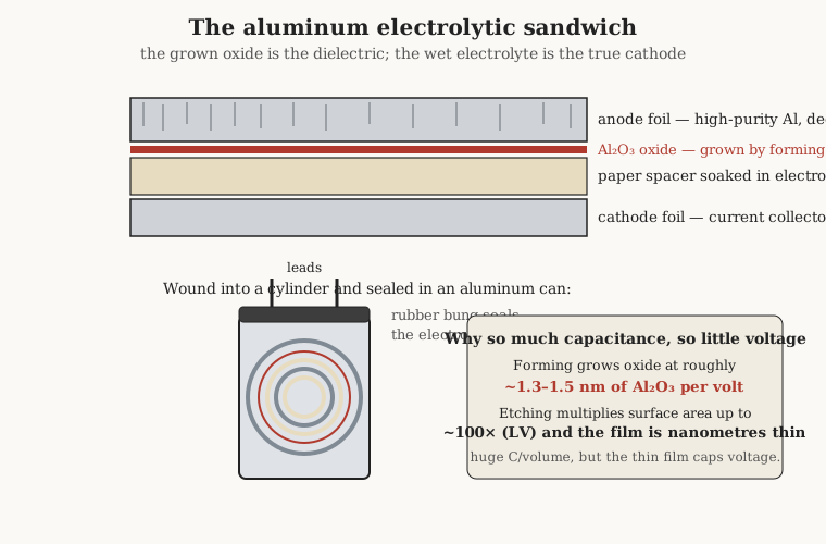
The wound element is impregnated with electrolyte, dropped into an aluminium can, and sealed with a rubber bung (an elastomer end seal) through which the leads pass. That seal is both the part’s lifeline and its Achilles’ heel: it keeps the electrolyte in, but over years and heat the electrolyte slowly escapes through it, and when enough has gone the capacitor dries out and its capacitance falls and ESR climbs — the ordinary end-of-life the endurance ratings predict. A final aging step applies rated voltage to heal any weak spots in the oxide, self-repairing small defects by growing a little more oxide exactly where the leakage is highest, before the part is tested and marked.
Modern variants swap the wet electrolyte for a solid conductive polymer, which has far lower resistance and does not dry out the same way, giving the low-ESR polymer and hybrid electrolytics the electrolytics volume covers — but the anode is made by the same etch-and-form process. The etch-and-form idea is the durable invention; the counter-electrode is negotiable.
4.6 Tantalum: the sintered sponge
Tantalum capacitors push the “roughen the surface” trick to its logical extreme. Instead of etching a foil, the maker starts with tantalum as a fine powder. That powder is pressed around a tantalum lead wire into a small pellet — loosely packed, only partly dense — and then sintered under high vacuum at a fierce temperature, broadly in the 1500 to 2000 °C range for a few tens of minutes. The heat welds the powder grains to one another at their contact points without fully melting them, producing a rigid, mechanically strong, electrically continuous porous pellet — a metal sponge riddled with interconnected voids. The vacuum sinter also purifies the tantalum, driving off absorbed oxygen from the grain surfaces. The payoff is internal surface area out of all proportion to the pellet’s size: a sponge has vastly more surface than a solid block of the same volume, and that hidden internal area is what the dielectric will coat.
From there the tantalum follows the electrolytic script. The sintered pellet is anodized — formed — in an electrolyte, growing a conformal skin of tantalum pentoxide, Ta₂O₅, over the entire internal surface of the sponge; this oxide, up to somewhat above a micron thick at high formation voltages, is the dielectric. Then the counter-electrode has to be worked into all that internal porosity, and here tantalums split into two families. The classic solid tantalum uses manganese dioxide (MnO₂): the pellet is repeatedly dipped in manganese nitrate solution and baked at a few hundred degrees, each cycle pyrolising a little more nitrate into solid MnO₂ that lines the pores, until a continuous MnO₂ cathode has grown throughout the sponge. Modern low-ESR parts instead impregnate the pores with a conductive polymer cathode. Either way the pellet is then coated with graphite and then silver to make external contact, attached to a leadframe, and moulded into an epoxy chip.
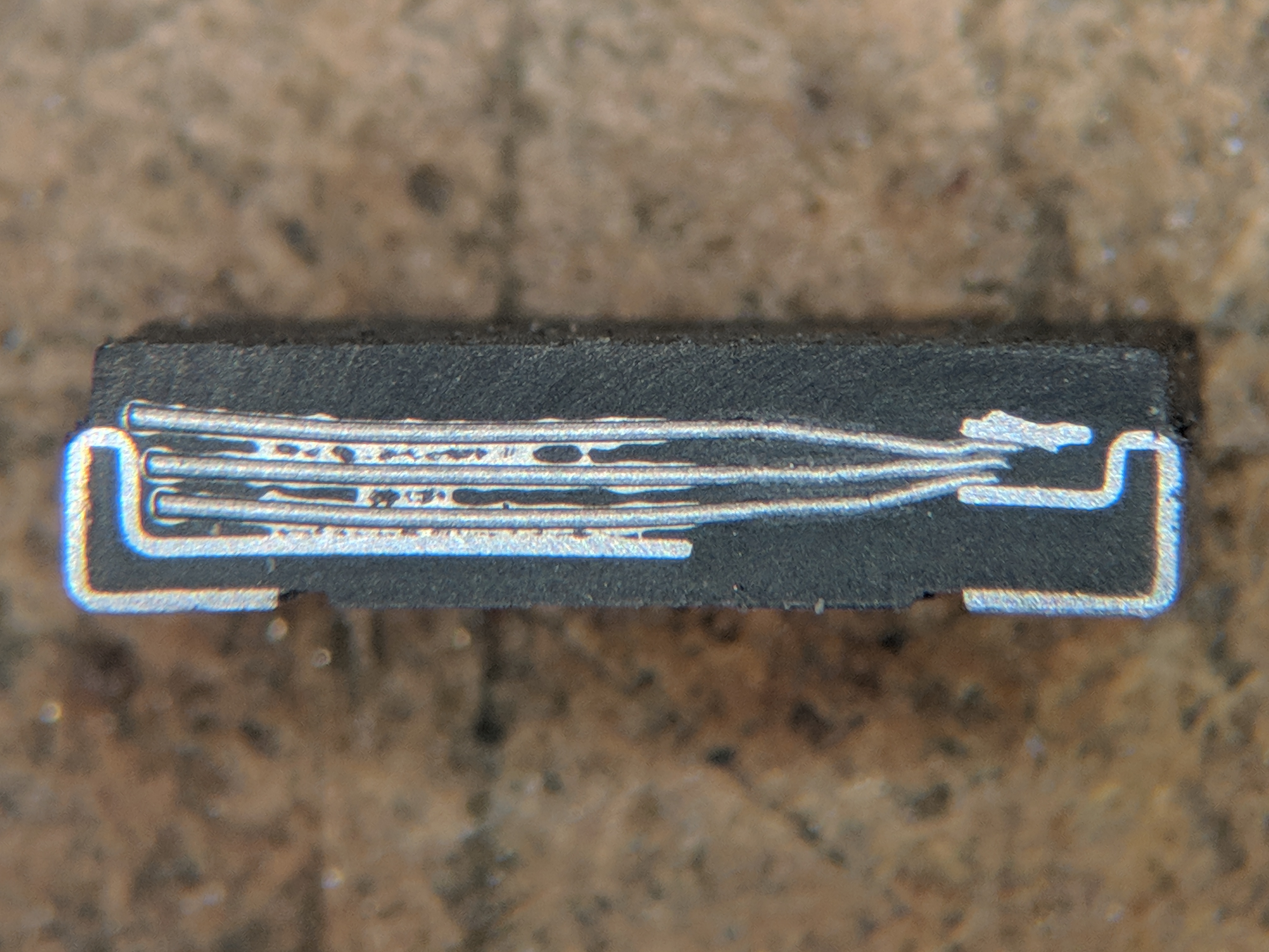
The sintered-powder route is the reason tantalum offers so much capacitance in so small and stable a package: a pressed pellet a couple of millimetres across contains an internal surface area that a rolled or stacked construction could never fit in the same volume, and the oxide over it is only nanometres thick. The tantalum volume covers the price of that density — the abrupt, sometimes incendiary failure mode when the MnO₂ version is over-stressed, and the derating rules that keep it in check — but the manufacturing insight is simply that a sponge beats a sheet when you need area.
4.7 Film capacitors in detail
Returning to the rolled world, it is worth walking the film capacitor’s own line, because it shows how the general wound geometry is refined into a precision part. It begins with the dielectric itself being made: molten polymer — PET or PP — is extruded and then stretched, often biaxially (in both directions), into a film only a few microns thick, thinner than kitchen cling wrap and far more uniform. For a metallized part, that film runs through a vacuum metallizer, where evaporated aluminium or zinc condenses onto it in a controlled pattern — the metallizers can even vary the coating thickness across the width, leaving a heavier “heavy edge” where the schoop will later contact and a lighter coating elsewhere to favour clean self-healing.
The metallized film is then wound — either into cylinders that are later flattened, or, for surface-mount chip film capacitors, wound onto a large drum and the whole drum’s worth cut into many rectangular stacked-film chips at once. The wound or stacked element gets its end spray (the schoop) on both faces to contact the electrodes, then leads or terminations are attached. Finally the element is flattened, taped, boxed, or potted in resin, and the box is filled and sealed against moisture — a real concern, since a thin polymer film offers little barrier and absorbed water degrades the dielectric. The film volume explains where each polymer and each construction wins; the manufacturing takeaway is that the film capacitor is the old paper-and-foil roll, refined by better dielectrics, vapour-deposited electrodes, and the self-healing they enable.
4.8 Mica and silver mica: the postage stamps
One more classic deserves mention because its process is unlike all the others: the mica capacitor. Mica is a natural mineral that cleaves into extraordinarily thin, flat, chemically stable sheets — a genuinely excellent dielectric handed over ready-made by geology. In the modern silver-mica construction, thin cleaved mica sheets are silvered: a silver paste is screen-printed onto each face and fired to fuse a metal electrode directly to the mica, replacing the older method of clamping mica between separate metal foils (which trapped tiny, unstable air gaps). The silvered sheets are then stacked in parallel to reach the wanted capacitance, leads are attached to the two sets of electrodes, and the stack is moulded in plastic or dipped in epoxy — the small, flat, rectangular “postage-stamp” capacitors of vintage RF gear. Because the dielectric is a natural crystal of superb stability and low loss, silver-mica parts hit tight tolerances and hold their value across temperature better than almost anything, which is why the specialty volume still reaches for them in precision RF work despite their cost and modest capacitance.
4.9 Where processes become field failures
A recurring theme across every one of these processes is that a capacitor’s reliability is very largely decided at the factory, and its eventual failure signature is usually a defect from the line grown up over years of service. This is worth stating plainly because it ties the manufacturing to the bench.
Cleanliness and moisture control dominate. A single contaminant particle embedded in an MLCC’s sub-micron dielectric, or a void left by imperfect lamination, is a built-in weak spot that can puncture in service; this is why MLCC lines are obsessive about filtered slurries and particle-free handling, and why the parts are often burned in — held at elevated voltage and temperature — to provoke the marginal ones into failing at the factory rather than in the field. In electrolytics, the health of the grown oxide and the integrity of the end seal set the lifetime, and a batch made with a flawed electrolyte formula can carry a latent defect that only shows up years later — the mechanism behind the early-2000s “capacitor plague” the electrolytics volume recounts. In tantalums, any weak spot in the Ta₂O₅ where the sponge sintered imperfectly becomes the site of the type’s characteristic surge failure. Even mechanical handling matters: the flex crack that kills an MLCC is not a material flaw at all but a manufacturing-and-assembly stress, born when a brittle monolith is soldered to a board that later bends.
The general lesson is that these components have no moving parts and, in principle, no wear-out — and yet they fail, because the thing being manufactured is a controlled near-flaw: a dielectric made as thin as the maker dares. Reliability is the art of keeping that deliberate thinness free of the defects that would let it break down. The measurement volume closes the loop, showing how a rising leakage or ESR on the bench betrays exactly these process defects maturing into failures.
4.10 Then versus now
Set the two eras side by side. In the 1930s, a capacitor for a radio was wound by a person: a strip of tin foil, a strip of tissue paper, another of foil, another of paper, spun onto a mandrel, dipped in molten wax, sealed, and marked with a loose tolerance and a colour code the reading volume decodes. It was bulky, it was made in the dozens or hundreds per operator, its value drifted, and within a few decades it would leak enough to need replacing — the recapping the paper volume is about.
Today, a capacitor for a phone is a fired ceramic monolith of several hundred sub-micron layers, made by the trillion, tumbling off a reel to be placed by a machine that positions dozens per second onto a board, at a tolerance and a price the wax-paper era could not have conceived — an 0201 chip costs a small fraction of a cent and holds more capacitance than a part a thousand times its volume once did. And yet the physics on the two benches is identical. Both are the same opening sentence — conductor, thin dielectric, conductor, as much area and as little thickness as the maker can manage — and both are solving the same optimisation. What changed across ninety years is not the idea but the execution: the dielectrics got thinner and better, the electrodes went from hand-wound foil to vapour-deposited films and sub-micron printed metal, the surfaces learned to explode into sponges and tunnels, and the economics went from an operator winding one part to a co-firing furnace and a pick-and-place head turning out more capacitors in an afternoon than the entire 1930s produced in a year. The family volumes that follow describe how each of these constructions behaves; this one has described how each is born, and the two together are what separate the datasheet from the part in the hand.
Comments (0)